
ADEKA Expands Production Capacity for Photoacid Generators Used in Advanced Photoresists for EUV Lithography
- Responding to Strong EUV Demand and Accelerating PAG Monomer Scale-Up -
Aug. 20, 2026
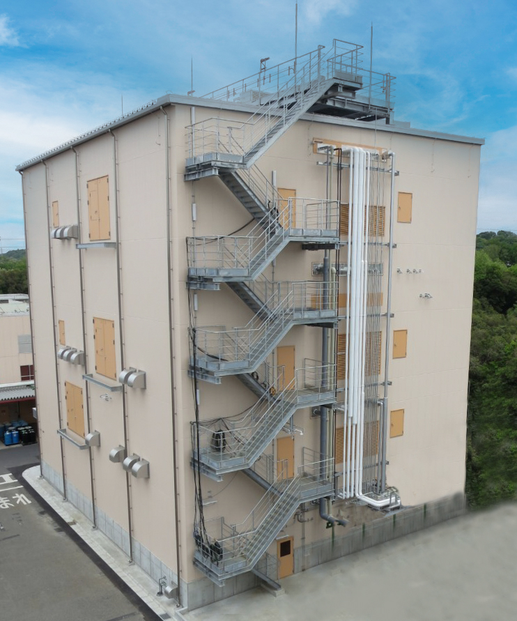
ADEKA Corporation hereby announces its decision to expand production capacity for photoacid generators (PAG) used in semiconductor photoresists for advanced semiconductor lithography processes, including extreme ultraviolet (EUV) lithography. The Company will add a new production line within an existing building at its Chiba Plant (Sodegaura City, Chiba Prefecture), with commercial operation scheduled to commence in September 2028.
As semiconductors have become strategic materials in today's global economy, investments in the industry continue to accelerate worldwide. The semiconductor market is expected to expand to approximately US$1.5 trillion by 2026, driving robust growth across the industry. In parallel, demand for photoresists, which are essential for semiconductor scaling, continues to increase. At the same time, advances in lithography technologies and environmental requirements, including the shift toward PFAS-free materials, are raising expectations for material performance and quality to unprecedented levels.
Within its semiconductor materials business, ADEKA has positioned advanced lithography applications requiring ultra-fine patterning technologies, such as ArF and EUV lithography, as a strategic focus area. The Company has been strengthening both development and supply capabilities for photoacid generators used in chemically amplified resists (CAR) and organometallic compounds for metal oxide resists (MOR).
This latest investment will increase production capacity for photoacid generators used in EUV lithography , for which demand remains strong, while further optimizing manufacturing operations under stringent metal contamination control standards at the 1 ppb level. At the same time, ADEKA's Semiconductor Innovation Center (Kuki City, Saitama Prefecture), which began full-scale operations in July 2026, is accelerating the development of PAG monomers (polymer-bound PAGs) for advanced technology generations, including EUV and High-NA EUV lithography. Through this investment, ADEKA will strengthen its supply capabilities to meet future demand, bringing forward these efforts by two years.
Going forward, ADEKA will continue to drive innovation in advanced lithography technologies through the dual pillars of photoacid generators for advanced photoresists and metal compounds for MORs, while further expanding its semiconductor materials business.
Outline
Investment Details |
Expansion of production facilities for Photoacid Generators |
|---|---|
Location |
ADEKA Chiba Plant (Sodegaura City, Chiba Pref., Japan) |
Investment value |
About 1 bllion yen |
Production Capacity |
Approximately 2× the current capacity |
|
Schedule |
Starting construction : Jan. 2027, |
For further information, please refer to the news release below.