Construction of a New Plant for Organometallic Compounds for MOR used of Next-Generation EUV Lithography
Oct. 31, 2025
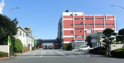
ADEKA has decided to construct a new plant for organometallic compounds for MOR used of Next-Generation EUV Lithography (High-NA EUV) at Kashima Chemicals Plant (Kamisu City, Ibaraki Prefecture).
Semiconductors, essential for realizing an advanced ICT society, are progressing toward high integration and high stacking due to the need for faster information processing and reduced power consumption. In this context, the lithography process, which forms fine circuit patterns by applying photoresist on silicon wafers and exposing them to light, is expected to see the full-scale introduction of "High-NA EUV." This technology enhances the resolution of exposure by expanding the lens aperture of EUV exposure equipment, enabling the formation of finer patterns to meet the further miniaturization of memory (HBM) and logic ICs.
With the introduction of High-NA EUV, a game change in photoresists used in the exposure process is required. It is anticipated that the adoption of a new concept photoresist, "MOR (metal oxide resist)," will expand alongside the currently mainstream CAR (chemically amplified resist).
The organometallic compounds for MOR produced at our new plant are key materials that improve EUV absorption and etching resistance of photoresists. They were made into products by applying metallic complex technology, which is indispensable for creating high-k materials for advanced memory. We have already started mass production at the Kashima Chemicals Plant and have begun supplying to customer. Now, with an eye on the full-scale introduction of High-NA EUV exposure, we are proceeding with the construction of a dedicated plant for organometallic compounds. The plant will have space reserved for future expansion to respond to a significant increase in demand and will also consider the production of new materials aimed at technological innovation in next-generation lithography processes, including High-NA EUV exposure.
The ADEKA Group contributes to the high performance of semiconductors with numerous advanced materials, including high-k materials (ALD materials) for advanced semiconductor memory and photoacid generators for EUV and ArF exposure used in CAR. In January 2026, a new research building will be completed within the Kuki R&D center (Kuki City, Saitama Prefecture), further strengthening the development system for ALD materials, photoacid generators for CAR and organometallic compounds for MOR.
ADEKA will continue to lead technological innovation in advanced lithography processes with materials, aiming to capture the world's top share in advanced materials for CAR and provide unique organometallic compounds for MOR recognized worldwide.
Outline
Location |
Kashima Chemical Plant (Kamisu City, Ibaraki Prefecture, Japan) |
|---|---|
Investment value |
3.2 billion yen |
Total floor area |
1,050m² |
Schedule |
Construction start:April 2026
|
Link for reference
IR Documents ; Business strategy for semiconductor materials(held in Feb. 27,2025)
For details, please refer to the following news release (PDF).